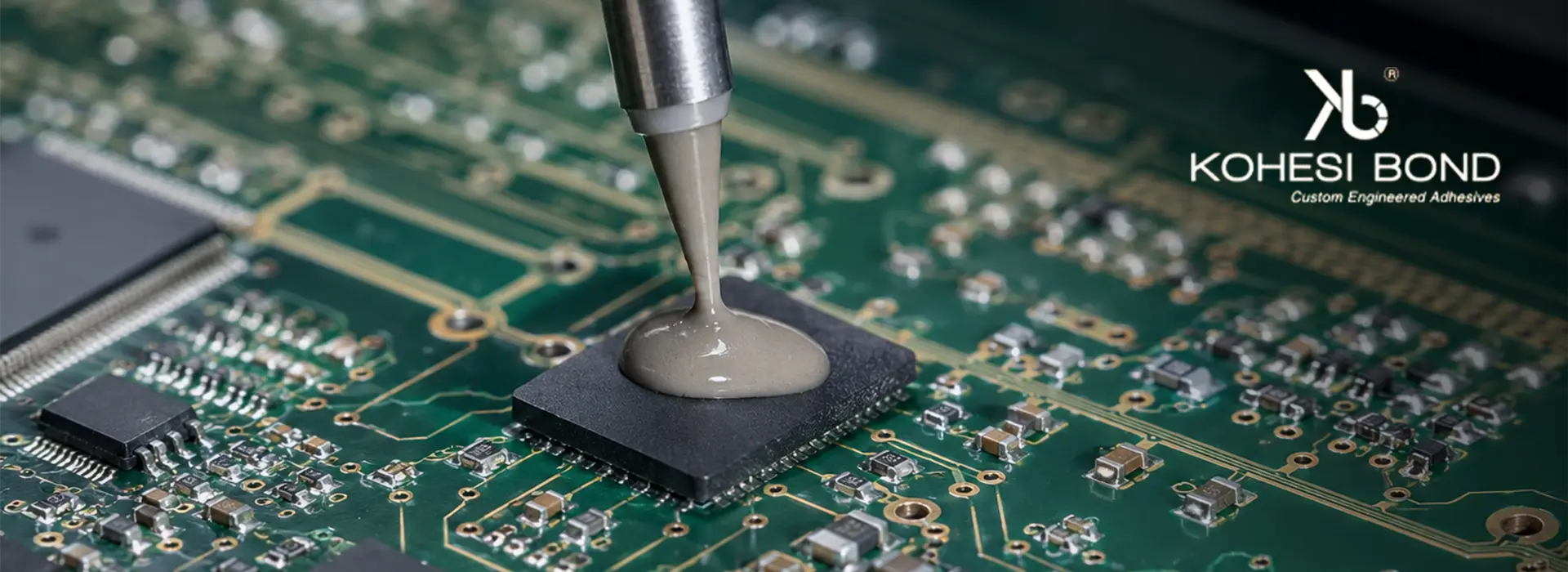
A ceramic capacitor on an automotive PCB survives 2,000 thermal cycles without incident, then develops a hairline crack at its solder joint during cycle 2,001. It showed no visual indication or any sign of immediate electrical failure. Just a fatigue crack propagating quietly through a rigid joint that was never designed to absorb 10 years of underhood temperature swings.
This is how PCB reliability fails in practice: not catastrophically, but progressively, at the interconnect.
Modern electronics have outpaced the joining methods built to assemble them. Component densities are higher, operating temperatures more extreme, and form factors tighter than the era that standardised reflow soldering. The joints connecting components to boards now carry mechanical, thermal, and environmental stress that solder was not engineered to handle indefinitely.
Conductive adhesive for PCB assemblies addresses these failure mechanisms directly, providing electrical interconnection and mechanical bonding in a single material that accommodates the physical demands of modern board design. Kohesi Bond engineers PCB conductive adhesive systems formulated for consistent conductivity, structural integrity, and long-term reliability across demanding operating environments.
Table of Contents
ToggleA] Reliability Challenges in Modern PCB Assemblies
1. Thermal Stress and Expansion Mismatch
Every material in a PCB assembly expands and contracts at a different rate. FR4 substrate runs at 14-17 ppm/°C in-plane, ceramic capacitors at 6-10 ppm/°C, and copper traces at 17 ppm/°C. Across thousands of thermal cycles, these mismatches generate cumulative interfacial stress that initiates cracking not in the component or the substrate, but precisely at the bond interface where stress concentrates. The demand for specialised electronics adhesives has grown as engineers seek joints that absorb what the materials cannot accommodate individually.
2. Mechanical Vibration and Shock
In automotive, aerospace, and industrial applications, PCBs experience continuous vibration and periodic shock loads. Rigid solder joints have limited capacity to absorb these inputs. Fatigue cracks initiate at joint edges under cyclic loading and propagate with each subsequent vibration cycle until the joint opens electrically, typically with no visible warning and no recoverable path except rework or replacement.
3. Miniaturisation and Fine-Pitch Components
Solder paste printing becomes unreliable below 0.3 mm pitch. Aperture clogging, insufficient fill, and bridging all increase in frequency as pad geometry shrinks. Assembly defect rates climb precisely as components become smaller, more densely spaced, and more expensive to rework or replace. This is where electrically conductive adhesives for microelectronic packaging provide a critical advantage, allowing for precise deposits that traditional soldering cannot achieve.
4. Environmental Exposure
Moisture ingress, temperature cycling, and chemical exposure degrade joint integrity progressively. In high-humidity environments, ionic contamination at joint interfaces drives leakage currents that compromise signal integrity before any mechanical failure occurs. Flux residues beneath low-standoff components accelerate electrochemical migration along signal traces, introducing resistance drift that standard continuity testing will not catch until the circuit has already degraded in the field.
B] Role of Conductive Adhesives in PCB Assembly
1. Electrical Interconnection
PCB assembly conductive adhesive creates conductive pathways through a network of metallic filler particles, typically silver, loaded above the percolation threshold within a cross-linked polymer matrix. Current flows through particle-to-particle contact across the bond line, achieving bulk resistivity in the range of 1×10⁻⁴ to 1×10⁻³ Ω·cm, depending on formulation and cure conditions.
2. Mechanical Bonding and Structural Support
Solder bonds only at the pad interface. Conductive epoxy for electronics adheres across the entire contact area between component termination and PCB pad, resisting both shear and peel forces across a distributed bond area. On fine-pitch and low-standoff components, where solder joint geometry is too small to provide meaningful structural support, this distributed adhesion is the difference between a mechanically stable assembly and one that fails its first drop test.
3. Stress Absorption and Vibration Damping
The viscoelastic nature of a cured epoxy matrix allows the bond line to deform elastically under mechanical load and recover, absorbing vibration energy rather than concentrating it at the joint edge. This is the fundamental mechanical advantage of polymer-based interconnects over solder under cyclic loading: the joint flexes rather than cracks. Furthermore, bond integrity is maintained through loading cycles that would initiate fatigue fracture in an equivalent solder joint within the first few hundred thousand cycles.
4. Compatibility with Fine-Pitch Assemblies
Electrically conductive adhesive can be jet-dispensed or needle-dispensed in deposits as small as 100-200 µm in diameter, enabling precise placement on 0201 components, fine-pitch BGAs, and chip-scale packages where solder paste printing produces bridging or insufficient fill. Deposit volume is controlled independently of pad geometry, eliminating the aperture ratio constraints that limit solder paste at small feature sizes.
Also Read: 10 applications of electrically conductive epoxy adhesives in the electronics industry
5. Kohesi Bond’s Approach
Kohesi Bond formulates silver conductive epoxy adhesive systems with controlled filler particle size distribution, optimised silver loading above the percolation threshold, and resin chemistry matched to the cure temperature constraints and mechanical requirements of each PCB application.
C] Advantages of Conductive Adhesives Over Traditional Interconnect Methods
1. Lower Processing Temperatures
Solder reflow peaks at 240°C-260°C. Conductive adhesive cure cycles operate at 60°C-120°C. For assemblies containing pre-calibrated sensors, thin-die semiconductors, or polymer substrates, this temperature difference determines whether the assembly survives the joining process with its performance intact. Conductive adhesive vs. soldering is not an abstract comparison; it is a practical choice between a process that protects the assembly and one that can potentially risk it.
2. Improved Stress Distribution
Where solder joints concentrate thermally and mechanically induced stress at their edges, adhesive bond lines distribute it across the full contact area. The governing relationship is:
σ_thermal = E × ΔCTE × ΔT
Where:
- σ_thermal = thermally induced stress at the bond interface (MPa)
- E = elastic modulus of the adhesive (GPa)
- ΔCTE = CTE difference between bonded materials (ppm/°C)
- ΔT = temperature differential experienced by the joint (°C)
Selecting an adhesive with lower elastic modulus E reduces σ_thermal directly, independent of the CTE mismatch between bonded materials. This is a design lever that solder does not offer.
3. Compatibility with Sensitive Components
Thermally conductive adhesive for PCB power component attachment and standard conductive adhesive for signal components both cure well below the thermal damage thresholds of MEMS sensors, thin-film passives, and pre-programmed processors. Components that would drift out of calibration during reflow or suffer junction degradation from thermal excursion remain stable throughout the adhesive cure cycle.
4. Enhanced Design Flexibility
Anisotropic conductive adhesive formulations conduct only through the bond line thickness in the Z-axis while remaining insulating in X and Y. This enables direct component-to-pad interconnection at ultra-fine pitch without bridging risk between adjacent pads, a capability that isotropic conductive adhesives and solder both lack below 0.2 mm pitch.
Need conductive adhesives that improve PCB reliability and electrical performance?
Trust Kohesi Bond for high-quality bonding solutions.
D] Key Performance Factors Affecting PCB Reliability
1. Electrical Conductivity and Contact Resistance
Initial bulk resistivity is only the starting point. A formulation measuring 5×10⁻⁴ Ω·cm at cure but drifting to 5×10⁻³ Ω·cm after 1000 hours at 85°C/85% RH has failed in service regardless of its initial specification. The relevant qualification dataset is resistivity after full environmental ageing, including 1000 thermal cycles between -40°C and +125°C and mechanical vibration per the applicable standard, not the as-cured value.
2. Adhesion Strength
Lap shear strength after environmental ageing is the meaningful adhesion metric. Bond surfaces in production are never perfectly clean, and adhesives must maintain structural integrity after realistic surface preparation quality and after the full environmental exposure the assembly will experience in service. As-cured strength on a pristine test substrate bears little relationship to in-service performance.
3. Thermal Stability
Glass transition temperature (Tg) must exceed the maximum operating temperature of the assembly with adequate margin. An adhesive with a Tg of 100°C operating continuously at 85°C in an underhood automotive location has only 15°C of headroom before the bond line softens and creeps under load. For most industrial and automotive PCB applications, Tg above 120°C is a practical minimum requirement.
4. Environmental Resistance
Moisture absorption into the cured epoxy matrix increases bulk resistivity, reduces adhesion strength, and drives electrochemical migration between adjacent conductive deposits. Moisture absorption rate and its effect on electrical properties must be part of the qualification dataset, specified and tested before production release rather than assumed acceptable after the fact.
E] Best Practices for Applying Conductive Adhesives in PCB Manufacturing
1. Surface Preparation
Pad surfaces must be free of oxides, flux residues, and handling contamination before adhesive application. ENIG-finished pads offer the most consistent adhesive interface. OSP-finished copper requires adhesive application within a controlled time window after oxide removal to prevent re-oxidation. Surface energy verification by contact angle measurement should be standard practice when process consistency is a qualification requirement.
2. Controlled Dispensing and Bond Line Thickness
Bond line thickness directly influences both electrical resistance and mechanical performance. Thicker bond lines increase the current path through the adhesive and raise bulk resistance; thinner lines reduce the viscoelastic stress absorption capacity that protects against vibration fatigue. A target bond line thickness of 25-75 µm balances these competing requirements for most component attach applications, with tighter control required for fine-pitch geometries.
3. Cure Profile Optimisation
A cure cycle that achieves handling strength but not full crosslink density leaves the bond line with degraded Tg, elevated resistivity, and reduced environmental resistance relative to specification. Cure temperature and time must achieve target crosslink density, confirmed by Tg measurement via DSC, and target resistivity, confirmed by a four-point probe on witness coupons cured alongside production assemblies.
4. Inspection and Testing
Four-point probe resistance measurement on test coupons verifies bulk conductivity after cure. Pull or shear testing on sample assemblies confirms bond strength against specification. Automated optical inspection before cure detects deposit placement errors and volume inconsistencies while correction is still possible. Post-cure electrical continuity testing confirms functional interconnection at the system level.
F] How Kohesi Bond Enhances PCB Reliability
1. Engineered Conductive Adhesive Formulations
Kohesi Bond’s electrically conductive adhesive systems are formulated for stable bulk resistivity and adhesion strength after full environmental ageing qualification. As a specialised high temperature adhesive manufacturer in India, our filler loading and particle morphology are co-optimised per application, ensuring the bond line remains stable even under extreme thermal loads.
2. Application-Specific Material Selection
The correct conductive adhesive for PCB application depends on the specific combination of substrate material, component thermal sensitivity, operating environment, and production process constraints. Kohesi Bond’s selection process maps each of these variables to formulation parameters, identifying the material that satisfies all requirements simultaneously rather than optimising one at the expense of the others.
3. Technical Support and Validation
Kohesi Bond provides dispensing parameter guidance, cure profile optimisation, and reliability testing support to move engineering teams from initial material selection to qualified production processes. Complete TDS, SDS, and CoC documentation accompanies every order, supporting quality system traceability requirements.
Conclusion
PCB reliability is a materials problem before it is anything else. As assemblies grow denser, operating environments grow harsher, and component thermal tolerances tighten, the interconnect material must absorb stress, protect components, and maintain its electrical and mechanical properties across years of thermal cycling, vibration, and environmental exposure. Solder was not designed for this combination of demands.
Conductive adhesives address each of these failure mechanisms directly. Kohesi Bond’s engineered formulations are built for the full performance envelope of modern PCB assembly. Contact our applications team to discuss your specific board, component, and operating environment.
Looking for dependable conductive adhesive solutions for your PCB applications?
Kohesi Bond delivers durable, precision-engineered adhesives.
FAQs
They replace or supplement solder as the electrical interconnect and mechanical bond between component terminations and board traces. In fine-pitch assemblies, MEMS sensors attach, and in any application where reflow temperatures would damage components or substrates, a conductive adhesive joint achieves the same electrical function at a cure temperature the assembly can actually survive.
By distributing mechanical stress across the full bond area rather than concentrating it at joint edges, adhesive interconnects resist the fatigue cracking that solder joints develop under thermal cycling and vibration. For a ceramic capacitor bonded to FR4, reducing joint modulus through adhesive selection directly reduces interfacial stress per the σ = E × ΔCTE × ΔT relationship, extending the number of thermal cycles the assembly survives before first failure.
Yes, specifically where reflow temperatures exceed component or substrate damage thresholds, where continuous vibration makes solder fatigue a predictable failure mode, or where fine-pitch geometry makes paste printing unreliable. For high-current power connections on robust, thermally tolerant substrates, solder remains the lower-resistance and lower-cost option. The choice should be driven by the specific failure modes the application faces, not by process familiarity.
Isotropic silver-filled epoxy systems conduct in all directions and are used for component attach, grounding, and die-attach. Anisotropic conductive adhesive formulations conduct only through the bond line thickness, enabling ultra-fine pitch interconnection without bridging risk between adjacent pads. The choice between them depends on pitch, pad geometry, and whether lateral insulation between adjacent bond deposits is a design requirement.
Start with the failure mode the adhesive must prevent: thermal fatigue, vibration-induced fatigue, or process-induced component damage. That determines whether low modulus, low cure temperature, or high Tg is the primary requirement. Then quantify the electrical specification, specifically resistivity after ageing rather than as-cured, and match viscosity and pot life to the dispensing method and production batch size. Kohesi Bond’s engineering team can map these requirements to a specific formulation with supporting qualification data.

Utsav Shah is a 34-year-old entrepreneur with a passion for scientific discovery. Utsav’s journey began with a deep dive into materials science, earning degrees from USC and the Institute of Chemical Technology. He’s the visionary founder of Kohesi Bond, a top-rated adhesive manufacturer, and Cenerge Engineering Solutions, a leader in heat exchangers and cryogenic pumps. With over a decade of experience, Utsav consults across various industries, ensuring they have the perfect adhesive solution for their needs. Connect with him on LinkedIn!